- 您现在的位置:买卖IC网 > Sheet目录673 > CA3162E (Intersil)IC CONVERTER A/D 3-DIGIT 16-DIP
�� �
�
�CA3162�
�Absolute� Maximum� Ratings�
�DC� Supply� Voltage� (Between� Pins� 7� and� 14)� .� .� .� .� .� .� .� .� .� .� .� .� .� .� .� +7V�
�Input� Voltage� (Pin� 10� or� 11� to� Ground)� .� .� .� .� .� .� .� .� .� .� .� .� .� .� .� .� .� .� .� ±� 15V�
�Operating� Conditions�
�Temperature� Range�
�CA3162E.� .� .� .� .� .� .� .� .� .� .� .� .� .� .� .� .� .� .� .� .� .� .� .� .� .� .� .� .� .� .� .� .� .� .� .� .� 0� to� 75� o� C�
�Thermal� Information�
�Thermal� Resistance� (Typical,� Note� 1)� θ� JA� (� o� C/W)�
�PDIP� Package� .� .� .� .� .� .� .� .� .� .� .� .� .� .� .� .� .� .� .� .� .� .� .� .� .� .� .� .� .� 90�
�Maximum� Junction� Temperature� .� .� .� .� .� .� .� .� .� .� .� .� .� .� .� .� .� .� .� .� .� .� .� 150� o� C�
�Maximum� Storage� Temperature� Range� .� .� .� .� .� .� .� .� .� .� -65� o� C� to� 150� o� C�
�Maximum� Lead� Temperature� (Soldering� 10s)� .� .� .� .� .� .� .� .� .� .� .� .� .� 300� o� C�
�CAUTION:� Stresses� above� those� listed� in� “Absolute� Maximum� Ratings”� may� cause� permanent� damage� to� the� device.� This� is� a� stress� only� rating� and� operation�
�of� the� device� at� these� or� any� other� conditions� above� those� indicated� in� the� operational� sections� of� this� specification� is� not� implied.�
�NOTE:�
�1.� θ� JA� is� measured� with� the� component� mounted� on� a� low� effective� thermal� conductivity� test� board� in� free� air.� See� Tech� Brief� TB379� for�
�details..�
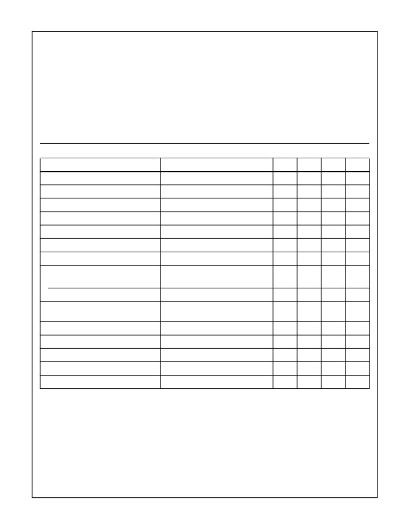
�Electrical� Specifications�
�T� A� =� 25� o� C,� V+� =� 5V,� Zero� Pot� Centered,� Gain� Pot� =� 2.4k� ?� ,� Unless� Otherwise� Specified�
�PARAMETER�
�Operating� Supply� Voltage� Range,� V+�
�Supply� Current,� I+�
�Input� Impedance,� Z� I�
�Input� Bias� Current,� I� IB�
�Unadjusted� Zero� Offset�
�Unadjusted� Gain�
�Linearity�
�TEST� CONDITIONS�
�100k� ?� to� V+� on� Pins� 3,� 4,� 5�
�Pins� 10� and� 11�
�V� 11� -V� 10� =� 0V,� Read� Decoded� Output�
�V� 11� -V� 10� =� 900mV,� Read� Decoded� Output�
�Notes� 1� and� 2�
�MIN�
�4.5�
�-�
�-�
�-�
�-12�
�846�
�-1�
�TYP�
�5�
�-�
�100�
�-80�
�-�
�-�
�-�
�MAX�
�5.5�
�17�
�-�
�-�
�+12�
�954�
�+1�
�UNITS�
�V�
�mA�
�M� ?�
�nA�
�mV�
�mV�
�Count�
�Conversion� Rate�
�Slow� Mode�
�Fast� Mode�
�Conversion� Control� Voltage� (Hold� Mode)�
�Pin� 6� =� Open� or� GND�
�Pin� 6� =� 5V�
�-�
�-�
�0.8�
�4�
�96�
�1.2�
�-�
�-�
�1.6�
�Hz�
�Hz�
�V�
�at� Pin� 6�
�Common� Mode� Input� Voltage� Range,� V� ICR�
�BCD� Sink� Current� at� Pins� 1,� 2,� 15,� 16�
�Digit� Select� Sink� Current� at� Pins� 3,� 4,� 5�
�Zero� Temperature� Coefficient�
�Gain� Temperature� Coefficient�
�Notes� 3,� 4�
�V� BCD� ≥� 0.5V,� at� Logic� Zero� State�
�V� DIGIT� Select� =� 4V� at� Logic� Zero� State�
�V� I� =� 0V,� Zero� Pot� Centered�
�V� I� =� 900mV,� Gain� Pot� =� 2.4k� ?�
�-0.2�
�0.4�
�1.6�
�-�
�-�
�-�
�1.6�
�2.5�
�10�
�0.005�
�+0.2�
�-�
�-�
�-�
�-�
�V�
�mA�
�mA�
�μ� V/� o� V�
�%/� o� C�
�NOTES:�
�1.� Apply� 0V� across� V� 11� to� V� 10� .� Adjust� zero� potentiometer� to� give� 000mV� reading.� Apply� 900mV� to� input� and� adjust� gain� potentiometer� to�
�give� 900mV� reading.�
�2.� Linearity� is� measured� as� a� difference� from� a� straight� line� drawn� through� zero� and� positive� full� scale.� Limits� do� not� include� ±� 0.5� count� bit�
�digitizing� error.�
�3.� For� applications� where� low� input� pin� 10� is� not� operated� at� pin� 7� potential,� a� return� path� of� not� more� than� 100k� ?� resistance� must� be� provided�
�for� input� bias� currents.�
�4.� The� common� mode� input� voltage� above� ground� cannot� exceed� +0.2V� if� the� full� input� signal� range� of� 999mV� is� required� at� pin� 11.� That� is,�
�pin� 11� may� not� operate� higher� than� 1.2V� positive� with� respect� to� ground� or� 0.2V� negative� with� respect� to� ground.� If� the� maximum� input�
�signal� is� less� than� 999mV,� the� common� mode� input� voltage� may� be� raised� accordingly.�
�3�
�发布紧急采购,3分钟左右您将得到回复。
相关PDF资料
CAA1M
LEVER ACTUATOR SNAP-ON MOUNTING
CAPW2BBP
CAP LIGHT 3-LED LITHIUM COIN
CBLK-300-3
DC BLOCK 300KHZ-3GHZ 16WVDC
CBPFS-0836
FILTER BAND PASS SAW 836.5 MHZ
CBPFS-0881
FILTER BAND PASS SAW 881.5 MHZ
CBPFS-0902
FILTER BAND PASS SAW 902.5 MHZ
CBPFS-0915
FILTER BAND PASS SAW 915 MHZ
CBPFS-1880
FILTER BAND PASS SAW 1880 MHZ
相关代理商/技术参数
CA3163
制造商:未知厂家 制造商全称:未知厂家 功能描述:Analog IC
CA3163 WAF
制造商:Harris Corporation 功能描述:
CA3164AE
制造商:未知厂家 制造商全称:未知厂家 功能描述:Industrial Control IC
CA3164AE WAF
制造商:Harris Corporation 功能描述:
CA3165
制造商:INTERSIL 制造商全称:Intersil Corporation 功能描述:Electronic Switching Circuit
CA3165E
制造商:INTERSIL 制造商全称:Intersil Corporation 功能描述:Electronic Switching Circuit
CA3165E1
制造商:Rochester Electronics LLC 功能描述:- Bulk
CA3166
制造商:Harris Corporation 功能描述: